SC417/SC427
23
Applications Information (continued)
grammed to 3.3V. After start-up, the device would connect
VOUT to VLDO and disable the LDO, since the two volt-
ages are within the ?00mV switch-over window. To avoid
unwanted switch-over, the minimum difference between
the voltages for V
OUT
and V
LDO
should be ?00mV.
It is not recommended to use the switch-over feature for
an output voltage less than 3V since this does not provide
sufficient voltage for the gate-source drive to the internal
p-channel switch-over MOSFET.
Switch-over MOSFET Parasitic Diodes
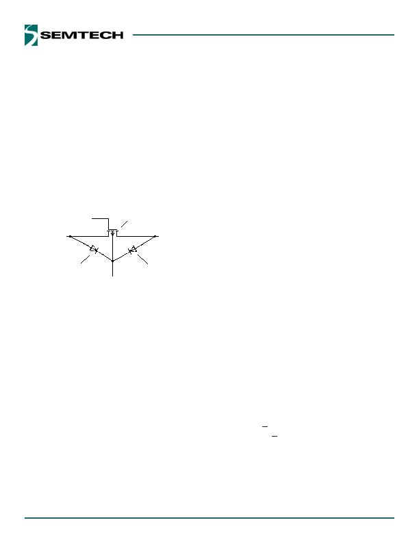
The switch-over MOSFET contains parasitic diodes that
are inherent to its construction, as shown in Figure 11.
Switchover
MOSFET
Parasitic diode
Parasitic diode
V5V
V
LDO
V
OUT
Switchover
control
Figure 11 Switch-over MOSFET Parasitic Diodes
There are some important design rules that must be fol-
lowed to prevent forward bias of these diodes. The fol-
lowing two conditions need to be satisfied in order for the
parasitic diodes to stay off.
V5V e V
LDO
V5V e V
OUT
If either V
LDO
or V
OUT
is higher than V5V, then the respective
diode will turn on and the SC417/SC427 operating current
will flow through this diode. This has the potential of
damaging the device.
Using the On-chip LDO to Bias the SC417/SC427
The following steps must be followed when using the on-
chip LDO to bias the device.
Connect V5V to VLDO before enabling the LDO.
The LDO has an initial current limit of 85mA at
start-up, therefore, do not connect any external
load to VLDO during start-up.
"
"
"
"
When VLDO reaches 90% of its final value, the
LDO current limit increases to 200mA. At this
time the LDO may be used to supply the required
bias current to the device.
Attempting to operate in self-powered mode in any other
configuration can cause unpredictable results and may
damage the device.
Design Procedure
When designing a switch mode supply the input voltage
range, load current, switching frequency, and inductor
ripple current must be specified.
The maximum input voltage (V
INMAX
) is the highest speci-
fed input voltage. The minimum input voltage ( V
INMIN
) is
determined by the lowest input voltage after evaluating
the voltage drops due to connectors, fuses, switches, and
PCB traces.
The following parameters define the design.
Nominal output voltage (V
OUT
)
Static or DC output tolerance
Transient response
Maximum load current (I
OUT
)
There are two values of load current to evaluate con-
tinuous load current and peak load current. Continuous
load current relates to thermal stresses which drive the
selection of the inductor and input capacitors. Peak load
current determines instantaneous component stresses and
fltering requirements such as inductor saturation, output
capacitors, and design of the current limit circuit.
The following values are used in this design.
V
IN
= 12V + 10%
V
OUT
= 1.05V + 4%
f
SW
= 250kHz
Load = 10A maximum
Frequency Selection
Selection of the switching frequency requires making a
trade-off between the size and cost of the external filter
components (inductor and output capacitor) and the
power conversion efficiency.
"
"
"
"
"
"
"
"
"
发布紧急采购,3分钟左右您将得到回复。
相关PDF资料
SE95D,112
IC SENSOR TEMP 2.8-5.5V SOT96-1
SE97BTP,547
IC TEMP SENSOR DIMM 8HWSON
SE98ATP,547
IC TEMP SENSOR DDR 8-HWSON
SG6901ASZ
IC PFC CTLR AVERAGE CURR 20SOIC
SG6932SZ
IC PFC CONTROLLER CCM 16SOP
SG6961SY
IC PFC CTRLR AVERAGE CURR 8SOIC
SI3500-A-GM
IC POE SWITCH PWR OVER LAN 20QFN
SI786LSG-E3
IC REG QD BUCK/LINEAR 28SSOP
相关代理商/技术参数
SC428
制造商:Mallory 功能描述:Sonalert
SC4-28
功能描述:SCREW 4-40 HEX .5"L FOR CONN MNT RoHS:是 类别:盒,外壳,支架 >> 卡架 - 配件 系列:VectorPak™ 标准包装:1 系列:VectorPak™ 附件类型:EFP 模块 适用于相关产品:PCB
SC428312CFGE
制造商:Freescale Semiconductor 功能描述:
SC42920FNR2
制造商:Motorola Inc 功能描述:
SC430769CFNER
制造商:Freescale Semiconductor 功能描述:SMOKE DETECTOR
SC430770CFNER
制造商:Freescale Semiconductor 功能描述:HEAT DETECTOR
SC431
制造商:SEMTECH 制造商全称:Semtech Corporation 功能描述:ADJUSTABLE SHUNT REGULATOR
SC431_05
制造商:SEMTECH 制造商全称:Semtech Corporation 功能描述:Adjustable Shunt Regulator